
Samsung develops ’12nm’ DDR5 DRAM as CPU DDR5 support widens
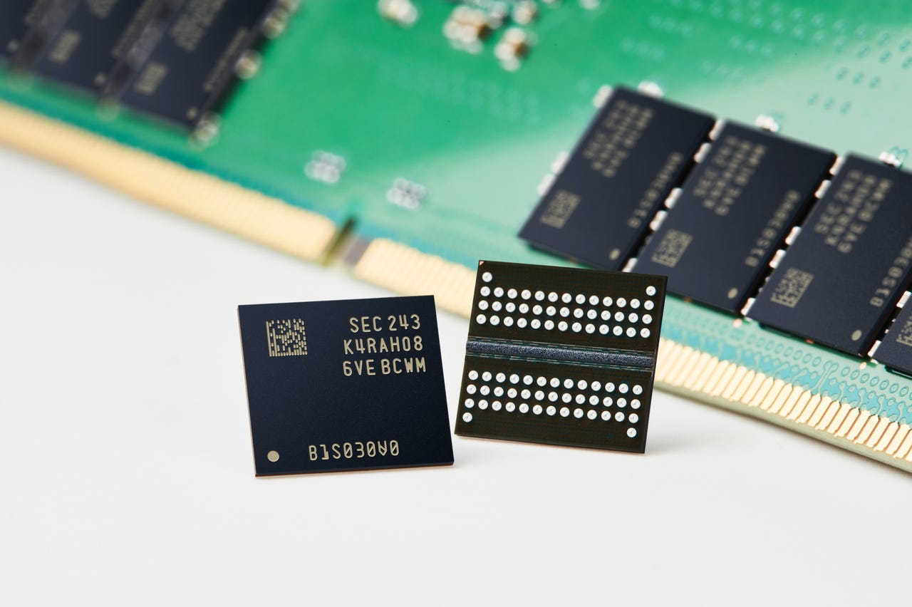
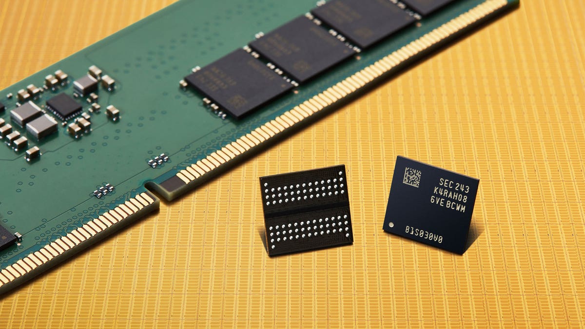
Samsung said on Tuesday that it has developed a double data rate 5 (DDR5) DRAM made with a 12-nanometer (nm) process node.
According to the South Korean tech giant, the 12nm 16Gb DDR5 DRAM has been verified with CPU maker AMD, with mass production slated to begin next year.
What is unusual about Samsung’s announcement is that it gave a specific numerical value of the process node it used __ in this case “12”.
Memory chipmakers, which includes SK Hynix and Micron, had mostly used the term “10nm class” or their own jargon for their process nodes ranging from 10 to 19nm in size without actually specifying their numerical value.
Samsung’s latest DRAM, to use its own term, is made with its fifth-generation 10nm process node. The tech giant is likely using 12nm this time around to tout how advanced it is over rivals’ 10nm class.
However, the actual transistor size and density between chips made by different companies, irrelevant of their process node names used for marketing, is difficult to know without testing and can differ greatly between each other.
On its 12nm 16Gb DDR5 DRAM, Samsung said it applied a new high-k material to increase the capacitor’s volume and applied new designs to complete the new process node. The tech giant said it also applied extreme ultraviolet (EUV) lithography to achieve the “industry’s highest” density.
Productivity has increased by 20% compared to the prior generation of the DRAM, which means more of them can be made per wafer.
The chip boasts a maximum speed of 7.2Gbps, which means it can process 60GB of data per second. Power consumption has been improved by 23% compared to its predecessor.
Samsung plans to launch more products in its 12nm DRAM range for applications in data centers, AI, and high-performance computing.